What is the manufacturing process for solar cells and solar panels ?
As we know, solar cells and solar panels are the core components in solar power system. In order to learn more solar panel, it is necessary to introduce how to produce solar cells and solar panel.
1. The working principle of solar cells.
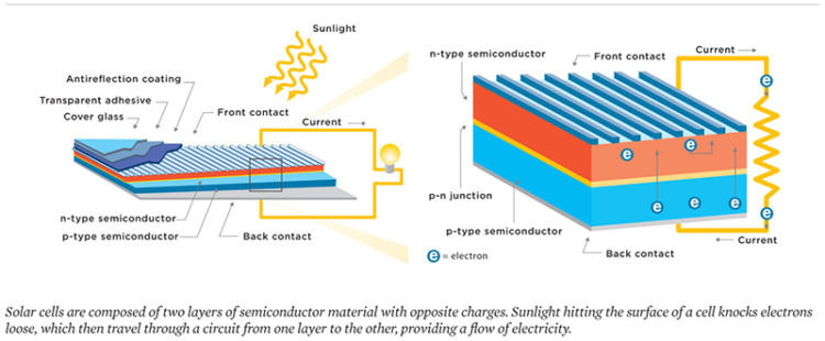
The solar irradiance radiates on the p-n junction of semiconductor to make up the new hole-electron pair, electron hole transmits from n field to p field under the electric field of p-n junction, it would produce current after processing circuit. This is the working principle of pv solar cells.
2. The manufacturing process of solar cells.
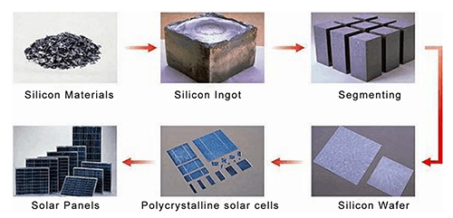
Usually, crystalline silicon solar cells are made by high quality silicon wafer whose thickness is 350~450um, this wafer is segmented to make from Tyra or Casting silicon ingot.
3. The manufacturing technique for solar cells.
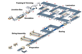
The manufacturing process of crystalline silicon solar cells is as below diagram.
It is the developing mainstream of solar cells technology to improve conversion rate of solar cells and decrease cost.

The specific manufacturing process is as below:
1) Slicing. To adopt multi-line cutting, cutting silicon rods into square wafer.
2) Cleaning. To use normal wafer cleaning method to clean, then use acid or alkali solution to wipe out 30-50um of cutting damage layer on the surface of silicon wafer.
3) Produce Suede. Use aqueous alkali to make various different erosion on the surface of silicon wafer to produce suede.
4) Phosphorus Diffusion. Adopt coated source or liquid source or solid nitrogen phosphor plate source to diffuse and produce PN+ junction, the deep of junction is about 0.3~0.5um.
5) Surrounding the corrosion. The diffusion layer which is formed on the surrounding surface of silicon wafer when making diffusion, would make short circuit on the top and bottom electron, need use masked wet corrosion or dry plasma etching to wipe out the surrounding diffusion layer.
6) Wiping out PN+ junction of backside. Usually, Wet Etching or Grinding Method are adopted to wipe out PN+ Junction of backside.
7) Making Top and Bottom Electrode. Use vacuum evaporation, chemical nickel-plating or aluminum slurry printing and sintering, to make the bottom electrode at first, then to make the top electrode. The aluminum paste printing is the technique which is the most adopted.
8) Making Antireflection Film. In order to reduce the loss of lighting reflection, it need cover a layer of antireflection film on the surface of silicon wafer. The materials which are being adopted to make antireflection film include MgF2, SiO2 , Al2O3, SiO, Si3N4, TiO2, Ta205, etc. The technique method includes Vacuum Coating, Ion Plating, Sputtering, Printing, PECVD or Spraying, etc.
9) Sintering. Sintering Cell Chip on the baseplate of nickel or copper.
10) The Test Step. Test to classify according to specified parameter specification.
4. The manufacturing process of solar panel.
Module line is also said as encapsulation line, encapsulation is the core process during production of solar module. Even better solar cells can’t produce better solar panel if don’t have better encapsulation technique. The encapsulation of solar cells not only can guarantee the lifespan of solar cells, but also can enhance the resistance ability. High quality and long lifespan products are the key factor to get clients’ satisfaction, so, the encapsulation quality of solar panel is very important.
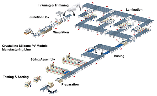
1) Solar Cells Test. As the manufacturing condition of solar cells is randomness, the cells performance has some difference, in order to group the solar cells which have the same or close performance, they need be classified according to their performance parameter. The cells test is to test their current and voltage, then classify them, to improve the use ratio of solar cells, then make quality conformance solar modules.
2) Front Welding. It is to weld bus bar on the frontside of solar cells (Positive Pole), busbar is tinning copper ribbon, the welding machine can weld solder ribbon on the main busbar by multipoint method. The hot source of welding is an infrared light ( it exploits the heat effect of infrared). The length of welding ribbon is about double length of cell side. The excessive solder ribbon connects with backside electrode of the next solar cell when welding on the backside.
3) Series connection on the backside. Backside welding is to series connect 60pcs solar cells to form a module series. The positioning of solar cells mainly rely on a mould plate, it has 60pcs grooves to put solar cells, the size of groove is relative with dimension of solar cells, the position of grooves have been set, different specification solar module need use different mould templates, The frontside pole (Negative) of solar cell would connect with the backside pole (positive) of the next solar cell, then connect 60pcs solar cells to form a solar module and outgoing line.
4) Laminated Laying. After completing back cascading and getting throng test, laying cells string, tempered glass, EVA, fiberglass and backboard according to certain layers, prepare to laminate. Tempered glass can be coated a layer of primer in advance to improve the bonding strength of glass and EVA. Need ensure the position of cells strings, glass and other materials when laying, to adjust the distance among solar cells, to create a good preparation for lamination. (From bottom to top, the layers of laying is tempered glass, EVA, solar cells, EVA, fiberglass, back sheet).
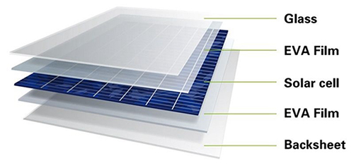
5) Module Lamination. Put the solar cells which have been laid into laminating machine, to extract air inside solar module to be vacuum, then heating to melt EVA to splice solar cells, tempered glass and back sheet. Finally, cooling and take out the solar module. Lamination technique is the key step of manufacturing module, the lamination temperature and time need be decided according to character of EVA. When expediting setting EVA, the lamination cycle time is about 25 minutes, the curing temperature is about 150℃.
6) Trimming. After laminating, EVA would extend outward to solidify and form rough edge, the rough edge need be wiped out after laminating.
7) Frame Up. To frame up solar module can improve the strength of solar module, furtherly to encapsulate solar module, to extend lifespan of solar cells. The gap between frame and glass can be filled up by silicone resin.
8) Soldering Junction Box. Soldering a box on the backside of solar module, which is good for solar cells to connect with electric devices.
9) High Voltage Test. High voltage test is to provide some voltage in the module frame and electrode lead, to test the resistance to pressure and dielectric strength of solar module, to guarantee the module can’t be damaged when working under severe natural condition.
10) Module Test. The purpose of test is to demarcate the power output of module, to test its output character, to confirm its quality grade. Presently, it mainly simulate solar irradiance to test under Standard Test Condition (STC), usually, the test time of a solar panel is about 7~8 seconds.
Above is the introduction for the manufacturing process of solar cells and solar panel, hope it could be helpful to learn more about solar power system, solar lighting belongs to a kind of solar system.
Bingsolar Power, 19th, January, 2018.
